-
Brad Bucher
Communications Lead, Manufacturing & Technology
Bechtel looks to offsite manufacturing, construction workforce development, supply chain buying power, and innovative construction sequencing to accelerate the design and build of new semiconductor fabs.
 Closeup shot of silicon microchip wafers. Image by Topaz Labs/Mohammad – stock.adobe.com.
Semiconductors, commonly called microchips, are a critical component of the electronics that power our daily lives, from smartphones, to cars, to household appliances.
An ongoing global chip shortage that started during the COVID-19 pandemic showed a sharp need to increase the resilience of the supply chain of chips. This has launched an increase in the construction of new semiconductor manufacturing facilities – known as “fabs” – in the U.S.
“Semiconductor makers want to build the facility as fast as they can, get the tools in, and start getting wafers out,” said Colin Featherstone, construction and startup sequence manager at Bechtel. “The quicker we can get them there, the better.”
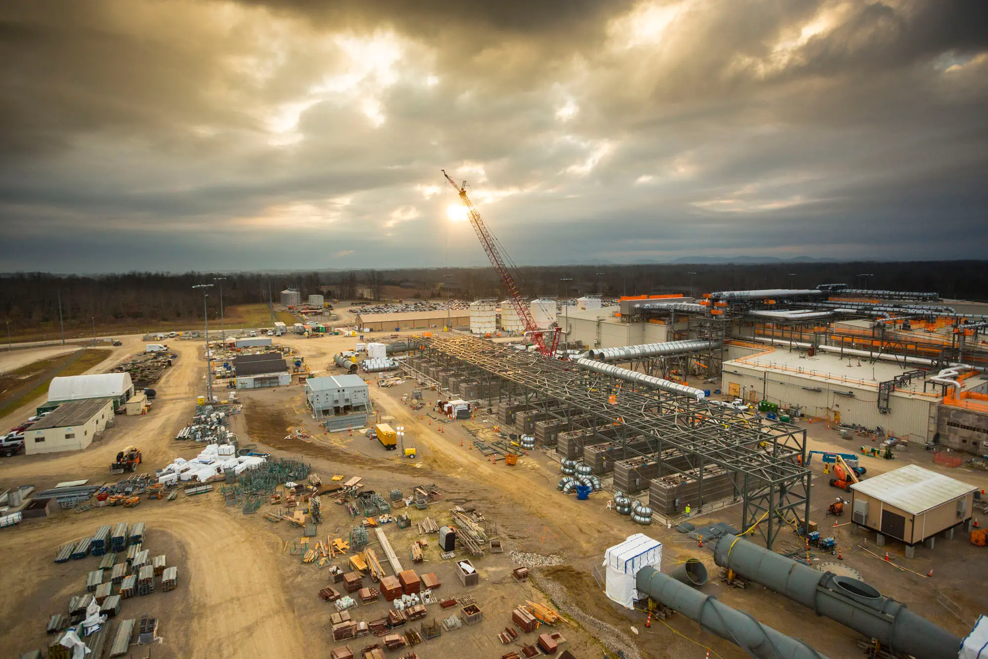
Designing and building a semiconductor fab is a multi-billion-dollar project with massive scale and complexity that takes years to complete. Bechtel is implementing strategies to accelerate these timelines, including offsite manufacturing, construction workforce development initiatives, supply chain buying power, and innovative construction sequencing.
Offsite Manufacturing
Offsite manufacturing is a construction approach to fabricate parts of a project as modules at different locations and then transport them to the final location for installation. The modules might include trestles for utilities, cabling, piping, or structural elements.
In one recent manufacturing project, Bechtel built 253 modules at four offsite module yards. Now, Bechtel is applying this approach to semiconductor projects using larger modules where possible along with hundreds of smaller modules.
“Offsite manufacturing allows us to work at many different sites in parallel,” said Neil Nunez, site manager at Bechtel. “The main jobsite could be constrained for space or resources. We can manufacture modules offsite and transport them in relieving local resource constraints.”
Construction Workforce Development
Semiconductor fabs are built to exacting standards that pose unique challenges for workers. Without previous experience on a semiconductor fab job site, the construction workforce may need preparation to maximize their productivity and safety.
“Craft professionals know how to build with conduit, cabling, and piping,” said Nunez. “But working in this type of an environment is a skill that needs to be developed. The difference is due to the extreme cleanliness required when manufacturing semiconductor facilities. We are building clean rooms that ultimately need to be cleaner than an operating room.”
Bechtel is partnering with unions to help develop the workforce for building semiconductor fab systems. For example, Bechtel is making updates to training facilities that emulate modules in semiconductor job sites.
“In one case Bechtel has designed mockups, purchased extra pipe, so it can be put it together at the pipefitters’ local training center,” said Nunez. “Craft professionals can give it a shot at the training center, so they aren’t experiencing the environment of a semiconductor fab for the first time on the job site. We also intend to send over field engineers to give craft professionals as much context as we can before they mobilize to the site and execute the direct work.”
Supply Chain Buying Power
“Understanding customer specifications early in the design process is important to getting in front of potential supply chain delays,” said Featherstone. “Everybody is chomping at the bit for specialty piping right now. New battery manufacturing projects are gearing up to power electric vehicles. Building battery manufacturing facilities requires a lot of the same materials as semiconductor fabs.”
Due to the massive quantities, materials for semiconductor fab projects might need to be ordered before early engineering is complete.
“Many materials required to build a semiconductor fab have lead times of over a year right now,” said Nunez. “But because Bechtel maintains a robust network of global suppliers and buys $15 billion worth of materials every year, we have relationships and buying power that can help our customers accelerate their timeline.”
Innovative Construction Sequencing
Bechtel experts are proposing new methods to segment semiconductor fab construction so they can be broken into smaller pieces.
“In simplified terms, fabs are usually built from one end to the other until the entire thing is complete,” said Featherstone. “Bechtel is working with fabricators on different approaches to build parts of the fab progressively, in different segments or gateways. The goal is to have the factory start to produce chips within a gateway while we are still completing and connecting the other gateways of the fab.”
Conclusion
Bechtel’s strategies offer a clear path for improved fab construction. Connect with Bechtel’s experts early to tap into their services for your next semiconductor fab project: www.bechtel.com/semi.
-
Brad Bucher
Communications Lead, Manufacturing & Technology


